





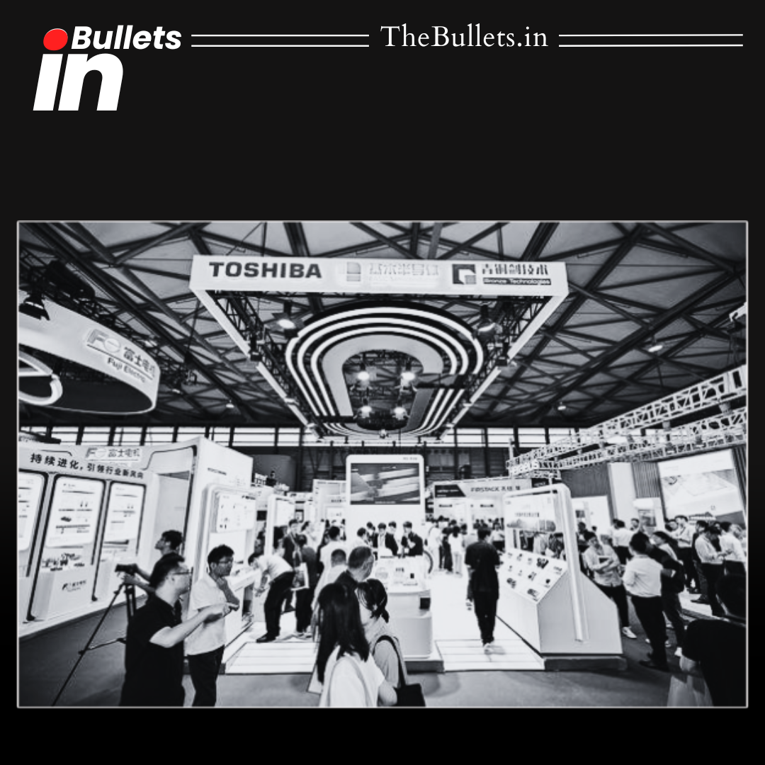


Prime Minister Narendra Modi inaugurated SEMICON India 2026 in New Delhi and rolled out Semicon 2.0, a ₹1,27,500 crore second phase of the India Semiconductor Mission aimed at moving the country beyond chip assembly into design, equipment, materials and research.
BulletsIn
- Prime Minister Narendra Modi inaugurated the fifth edition of SEMICON India 2026 at Yashobhoomi, New Delhi, on 17 September under the theme “Silicon to Systems: Building the Ecosystem.”
- The event formally launched Semicon 2.0, the second phase of the India Semiconductor Mission, with a Cabinet-approved outlay of ₹1,27,500 crore against ₹76,000 crore for Semicon 1.0.
- Semicon 2.0 extends government support across six pillars: chip design, machines and materials, fabs, advanced packaging, applied research and development, and talent.
- The India Semiconductor Mission functions as an independent business division under the Ministry of Electronics and Information Technology’s Digital India Corporation.
- The Prime Minister virtually inaugurated two new commercial production lines, CDIL Semiconductor in Mohali and Suchi Semicon in Surat, taking commercial units to five of the twelve approved under Semicon 1.0.
- India’s chip demand is projected to touch USD 110 billion by FY2030, even as the country still imports 90 to 95 percent of its semiconductor consumption, per NITI Aayog estimates.
- Eleven memoranda of understanding were signed at the event, most involving Tata Electronics, including agreements with Nexperia, Fujifilm and BESI covering wafers, materials and advanced packaging.
- Applied Materials announced a USD 5 billion “India Vision 2035” investment plan, while Lam Research committed roughly ₹10,000 crore to a silicon-component and ingot-processing plant.
- The government has set targets of training one lakh technicians over five years and supporting 200 semiconductor design start-ups under the new phase.
- All five commercially operating units remain in assembly, testing and packaging, the lowest value-added segment, while India’s first large wafer fab at Dholera is still under construction.
- The scheme builds on a policy stack that includes the Design Linked Incentive scheme, the Electronics Components Manufacturing Scheme and 100 percent FDI in electronics manufacturing under the automatic route.
- Semicon 2.0’s success will depend on whether announced investment commitments and design start-up targets convert into commissioned fabrication capacity rather than remaining assembly-stage gains.



What do you think?
It is nice to know your opinion. Leave a comment.